ملف:(Geometry of Nature) Геометрія природи.jpg
حجم هذه المعاينة: 800 × 600 بكسل. البعد الآخر: 1٬700 × 1٬275 بكسل.
الملف الأصلي (1٬700 × 1٬275 بكسل حجم الملف: 2٫74 ميجابايت، نوع MIME: image/jpeg)
وصف قصير
| Description |
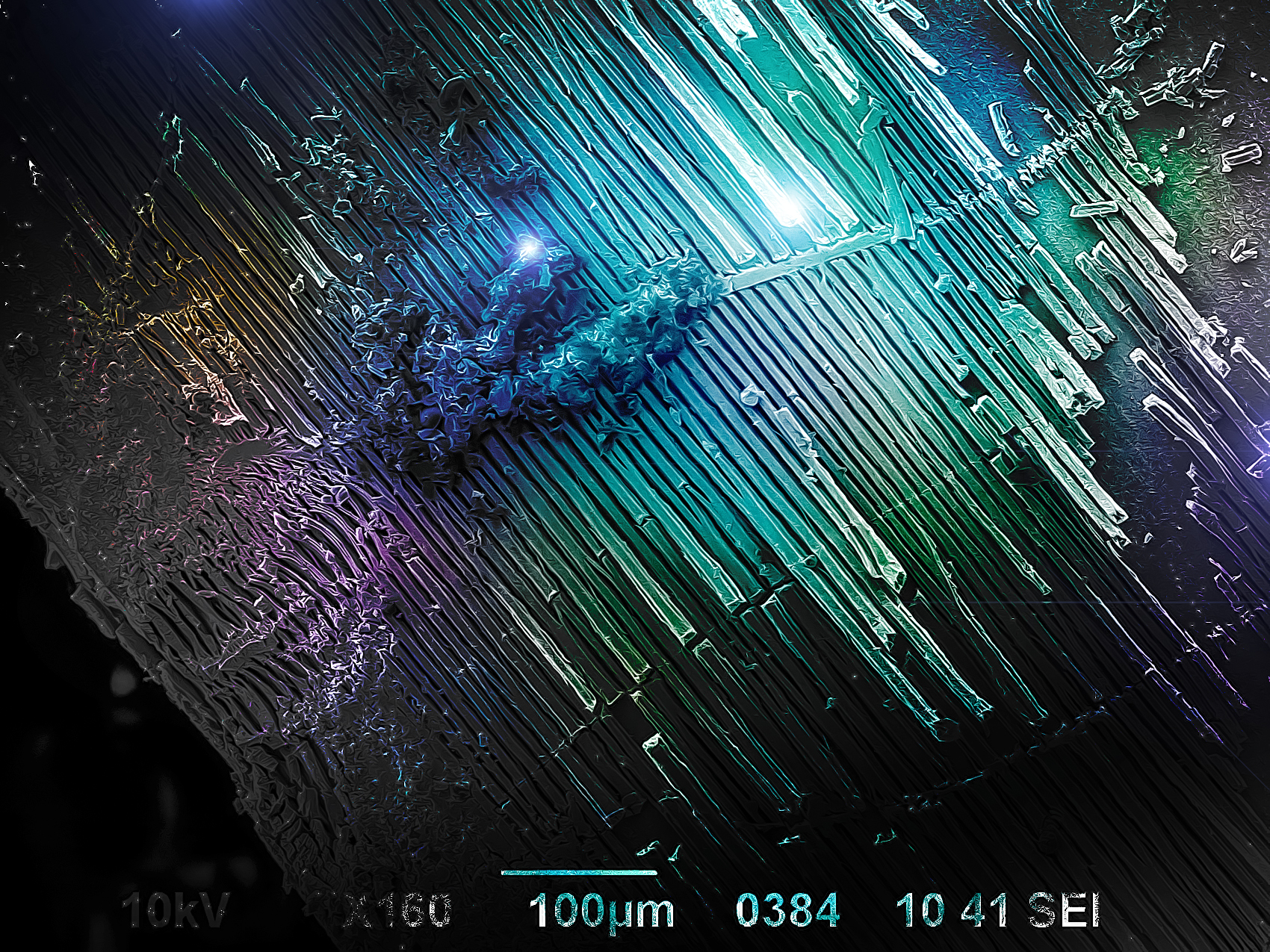
قالب:Uk English: The image of the morphology of the textured InP plate. Photos of nanostructures were obtained in scanning electron microscope JSM-6490 by the researchers of Berdyansk State Pedagogical University. Increased 160 times. Indium phosphide (InP) has great prospects of wide industrial production. Field-effect transistors and other microwave devices are manufactured based on InP. Monocrystalline InP plates are used as substrates for the growth of different heterostructures, which are the basis of effective radiation sources (injection lasers, light-emitting diodes) and high-speed photodetectors for the systems of fiber optic communication lines. InP is promising for the development of super-high-speed integrated circuits. Presently InP is the most probable material for the mass production of integrated circuits. It is impossible not to mention about the growing interest in porous InP, which has unusual optical and electrical properties in comparison with the monocrystalline InP. Such structures can find application in sensor (since their sensitivity depends on the surface area) and solar cell (possibility of the accumulation of a record amount of energy) manufacturing. |
| Date | 2015-10-27 11:58:21 |
| Source | Own work |
| Author | Яна Сычикова, Ковачев Сергей |
ترخيص
|
تاريخ الملف
اضغط على زمن/تاريخ لرؤية الملف كما بدا في هذا الزمن.
| زمن/تاريخ | صورة مصغرة | الأبعاد | مستخدم | تعليق | |
|---|---|---|---|---|---|
| حالي | ★ مراجعة معتمدة 15:51، 4 نوفمبر 2023 | | 1٬700 × 1٬275 (2٫74 ميجابايت) | Pastakhov (نقاش | مساهمات) | Upload https://upload.wikimedia.org/wikipedia/commons/1/14/%28Geometry_of_Nature%29_%D0%93%D0%B5%D0%BE%D0%BC%D0%B5%D1%82%D1%80%D1%96%D1%8F_%D0%BF%D1%80%D0%B8%D1%80%D0%BE%D0%B4%D0%B8.jpg |
لا يمكنك استبدال هذا الملف.
وصلات
لا يوجد صفحات تصل لهذه الصورة.
_Геометрія_природи.jpg&oldid=3370314)